Industria de semiconductores
El campo de batalla invisible en la fabricación de semiconductores: cómo una deformación de 0,2 μm puede inutilizar obleas por valor de $5 millones de dólares.
Un fallo en el sistema de vacío que costó cientos de miles de dólares se debe a una pequeña deformación invisible a simple vista.
En el mundo de la fabricación de semiconductores, se libra una batalla implacable a escala microscópica. Aquí, los adversarios son invisibles y el resultado de estas batallas se decide a nivel de micras o incluso nanómetros.
Cuando una máquina de litografía EUV multimillonaria pierde el vacío debido a una minúscula deformación en una puerta FOUP, o cuando se desechan obleas de 3 nm por valor de 1.540.500 millones de dólares debido a la contaminación por partículas, estos no son incidentes aislados, sino ejemplos extremos de los desafíos diarios en la fabricación de semiconductores de precisión.
En esta búsqueda de máxima precisión, los métodos de fabricación tradicionales ya no satisfacen las exigentes necesidades de los equipos para semiconductores. Como socio de proveedores como ASML, Lam Research y Applied Materials, Vanmodel Sheet Metal está redefiniendo los estándares de fabricación de componentes clave para equipos de semiconductores.
La precisión lo es todo: la revolución de la planitud en los equipos para semiconductores.
Una deformación de tan solo 1 μm/m² es suficiente para comprometer los sellos de vacío.—un requisito que se vuelve aún más crítico en procesos avanzados como la litografía ultravioleta extrema (EUV). Como contenedor principal para el transporte y almacenamiento de obleas dentro de las instalaciones de fabricación, el rendimiento de sellado del FOUP (Front-Opening Unified Pod) determina directamente el rendimiento de la línea de producción.
La causa principal suele residir en las tensiones internas del material.Los componentes de los equipos de semiconductores desarrollan tensiones internas durante el procesamiento, que se liberan con el tiempo, lo que provoca una deformación gradual durante el uso. Para abordar esto, implementamos un Proceso de envejecimiento térmico de 48 horas a 300 °C.estabilizando la estructura cristalina de la aleación de aluminio 6061-T651 en la fuente del material mediante el control preciso de la curva de temperatura, evitando así futuras deformaciones.
En el procesamiento de planitud, combinamos Tecnología de rectificado de superficies con detección por interferómetro láser lograr Planitud de 0,5 μmEste nivel de precisión equivale a variaciones no mayores que el diámetro de un cabello humano en un área del tamaño de un campo de fútbol, un estándar inalcanzable mediante los métodos de fabricación tradicionales.
La distorsión de la soldadura presenta otro desafío crítico. Nuestro Proceso de soldadura TIG pulsada con purga de argón Controla eficazmente el aporte de calor, minimizando la deformación durante la soldadura. Esta técnica garantiza que las puertas FOUP mantengan una excelente planitud de sellado después de la soldadura.
Control de la contaminación: Guardianes del rendimiento de los semiconductores
Los entornos de fabricación de semiconductores exigen un control de la contaminación extremadamente riguroso. Una sola partícula microscópica puede provocar la pérdida de obleas por valor de decenas de miles de dólares. Las investigaciones demuestran que la contaminación molecular dentro de los FOUP causa directamente defectos en las obleas, incluyendo problemas de crecimiento de cristales y corrosión de las interconexiones metálicas.
El control de las salas blancas constituye la primera línea de defensa contra la contaminación.. Nuestro Salas blancas de clase 5 garantizar que el recuento de partículas para la fabricación de componentes críticos se mantenga estrictamente por debajo de 3.520 partículas/m³—un estándar que supera con creces el de los entornos de fabricación convencionales.
La tecnología de tratamiento de superficies es igualmente crucial.. Nuestro El proceso de electropulido logra una rugosidad superficial de Ra<0,1 μm.Esto no solo reduce las áreas de adhesión de partículas, sino que también disminuye significativamente la tasa de desgasificación del material. Los estudios indican que un tratamiento superficial adecuado puede reducir la tasa de desgasificación del acero inoxidable y las aleaciones de aluminio varias veces.
En el tratamiento de pasivación, hemos adoptado un Proceso de pasivación con ácido cítrico respetuoso con el medio ambiente para sustituir la pasivación tradicional con ácido nítrico.Este cambio mantiene la eficacia de la pasivación en las superficies de acero inoxidable al tiempo que reduce sustancialmente el impacto ambiental, un cambio ampliamente reconocido por numerosos fabricantes de semiconductores.
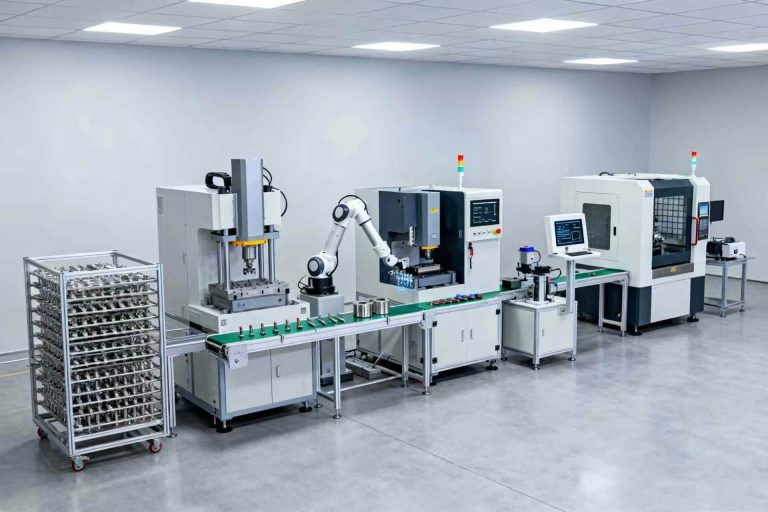
Del CAD a la fabricación: La ventaja de la velocidad en la innovación de semiconductores
En la industria de semiconductores, donde hay mucho en juego, El tiempo de comercialización es directamente proporcional a la cuota de mercado.La capacidad de iterar y validar rápidamente los diseños de componentes repercute directamente en la ventaja competitiva de nuestros clientes.
Hemos comprimido el ciclo de creación de prototipos de FOUP del estándar de la industria de 6 semanas a solo 10 días—desde el diseño CAD hasta la cápsula funcional. Esta aceleración es posible gracias a nuestro enfoque de fabricación integrado y Tecnología de desbarbado sin partículas mediante acabado abrasivo magnético (MAF)..
Nuestras capacidades de equipamiento incluyen:
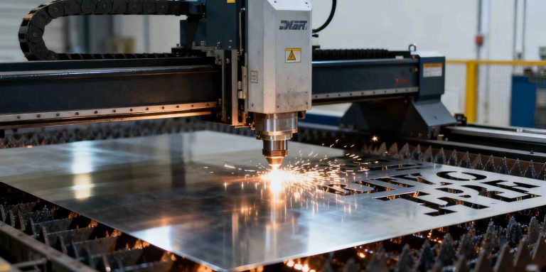
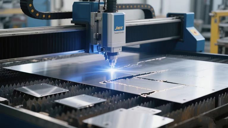
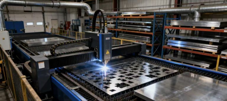
- Sistema de corte láser AMADA LC-3015 F1 de 6 kW con una precisión de ±0,03 mm
- Certificado Aluminio 6061-T651 y acero inoxidable 304/316L materiales con bajas propiedades de desgasificación
- Prueba de fugas de helio capacidades hasta 1×10⁻⁹ Pa·m³/s
Un fabricante de equipos para semiconductores lo confirmó: “Las puertas FOUP de Vanmodel mantuvieron un vacío inferior a <0,01 Pa durante más de 200 ciclos, cumpliendo con las especificaciones del fabricante original a un costo 40% menor.”
Conclusión: Precisión sin concesiones
En la fabricación de semiconductores, no hay margen para concesiones. Cada micrón, cada acabado superficial y cada elección de material tiene profundas implicaciones para el rendimiento final.
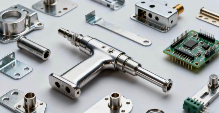
Vanmodel Sheet Metal trae precisión de grado semiconductor En cada componente que fabricamos, desde la selección y el procesamiento de los materiales hasta la inspección final, mantenemos estándares que cumplen o superan los requisitos de la industria.
Exija precisión de grado semiconductor
Descargue nuestra hoja de especificaciones de planitud FOUP
Vanmodel Sheet Metal: Componentes de precisión para la industria de semiconductores.
Proveedores de confianza para ASML, Lam Research y Applied Materials.